Solar Phone Charger
Jalius Welch
Design
The solar phone charger project is a senior design project that I completed as part of my Power Electronics II class. The assignment was to design a power electronic DC-DC converter that was capable of converting 20V from a solar panel to 5V 10W power that would be used to charge a phone via USB.
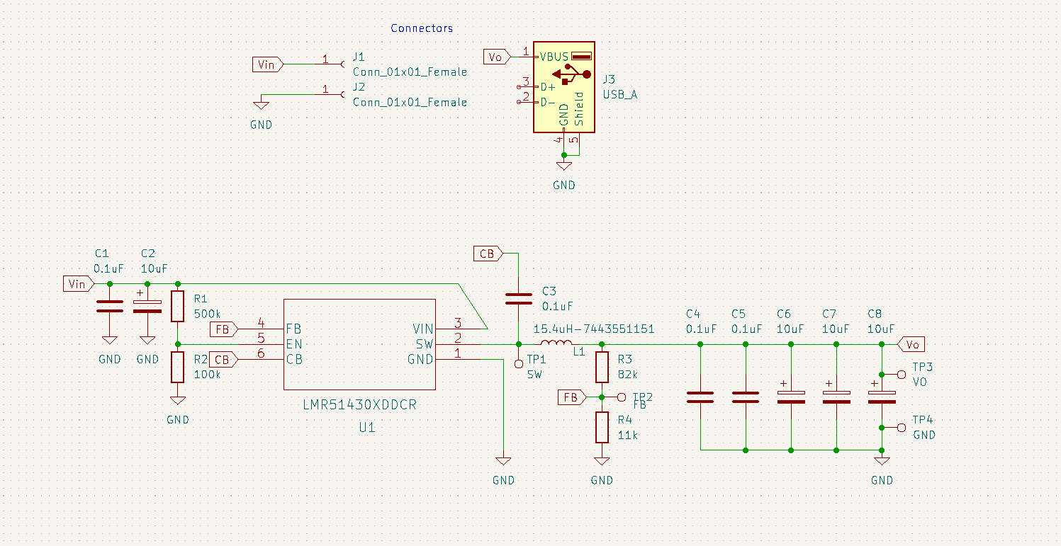
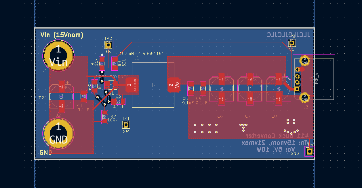
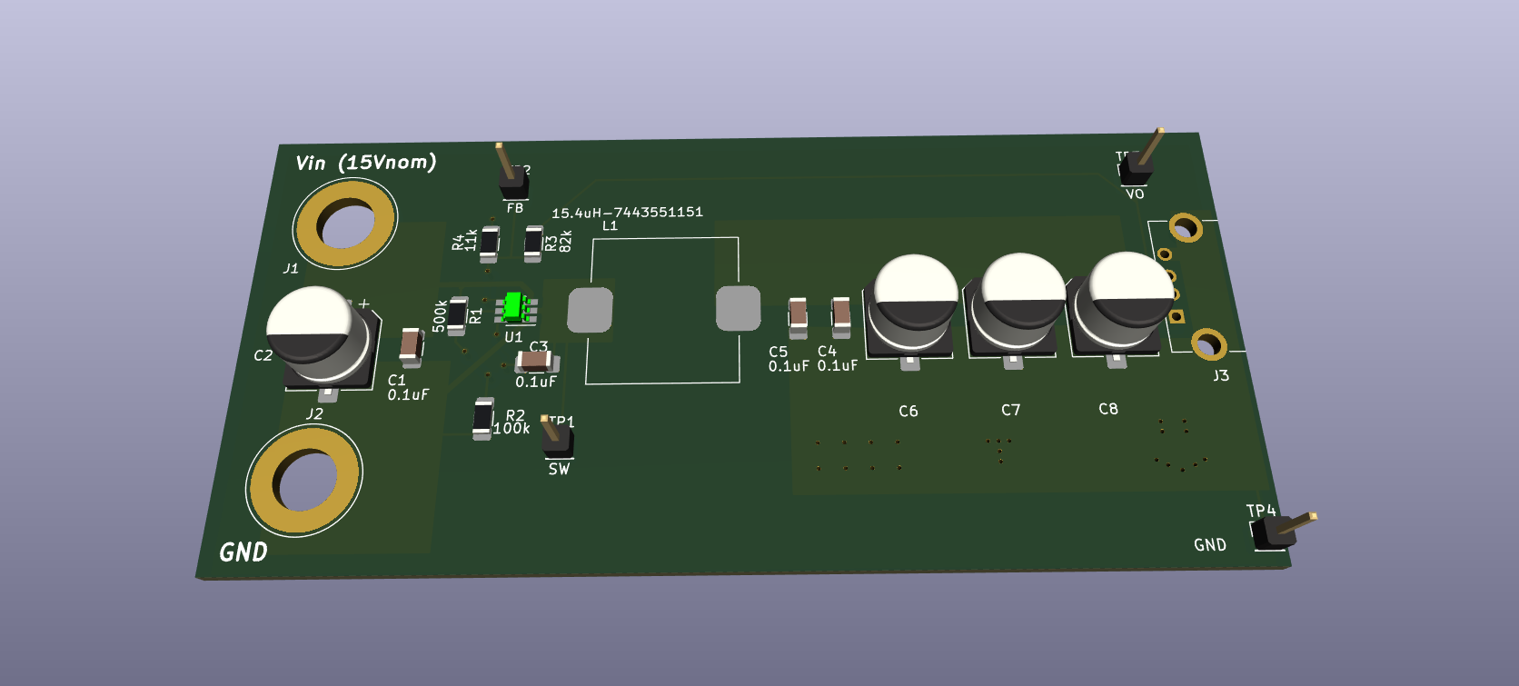
The board was constrained to 50mm x 100mm and the component packages were to be SMD. I selected a buck IC with PWM and internal switches, to reduce part count. The buck IC I selected also had an SOT23 package, which I selected over the smaller SOTs and BGA for the ease of hand-soldering for prototyping. This was the first time I've done layout for a high-frequency converter circuit, I followed the reference design from the buck-converter IC datasheet. This called for a straight shot between Vin and Vout, and large power tracks, to minimize inductance in the power path. I selected the remaining components to fit the design equations and recommendations in the buck's datasheet.
Production
After the layout was completed, I checked the net connections and trace widths, verified the design with my instructor and then sent the gerber and drill files to the board manufacturing plant.
The final board arrived, and I hand-soldered the components onto the board without too much trouble, and proceeded to test the connections. Once the board was assembled, I ran open circuit and loaded tests to confirm the circuit met the rated specifications.
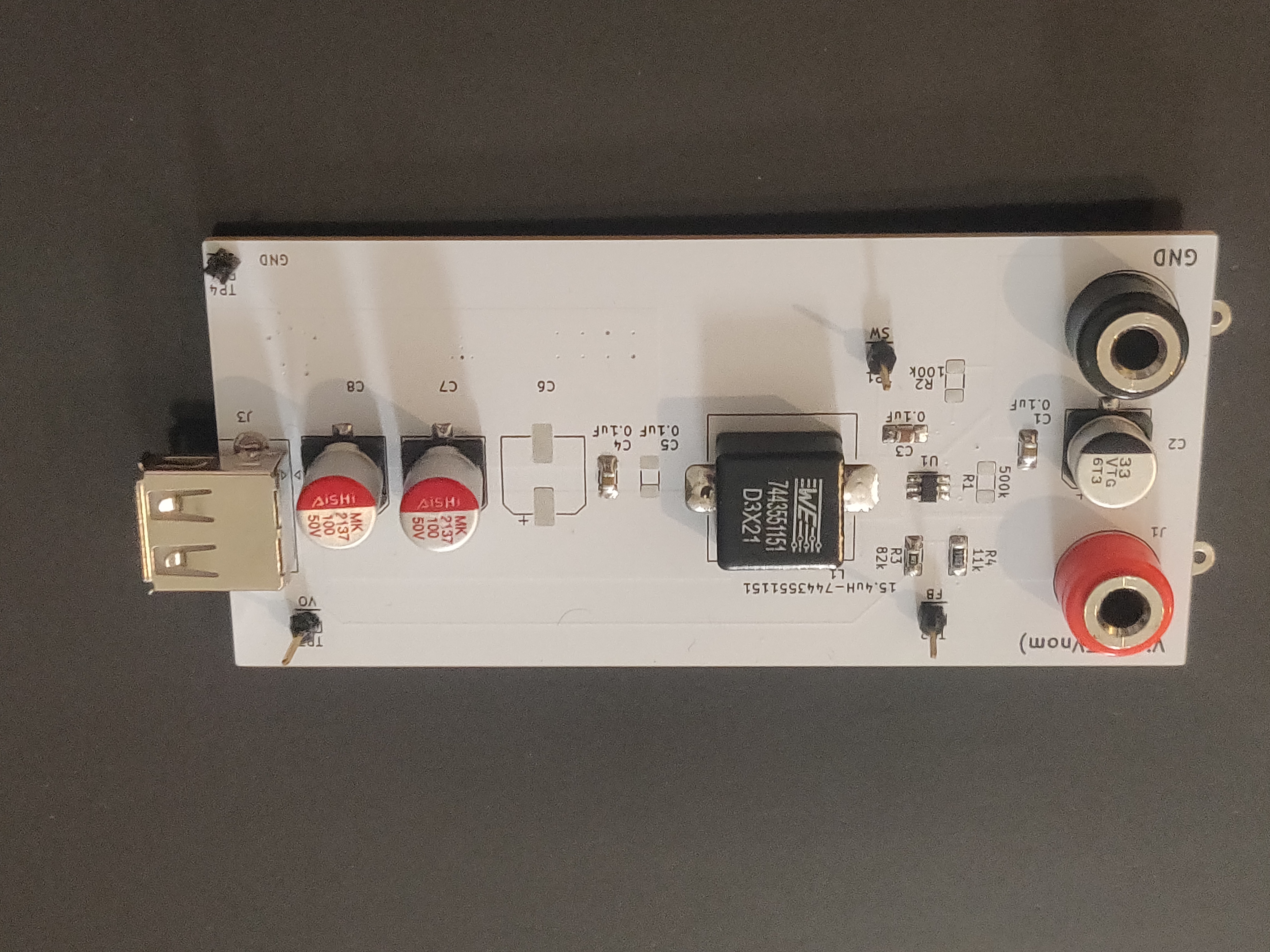
The board performed well in practical tests, and was able to charge a cell phone at 5V/250mA. The final board met all the specifications except for voltage regulation (coming in at 4%, over the specified 3%), while input and output voltages (22V in-max and 5V out), line regulation (<1%), and efficiency (87%) were met.